
The main idea behind a Digital LDO is the use of an array of small power transistors that operate as switches [figure 1]. The use of power transistors as switches facilitates low VDD power management and process scalability which makes Digital LDOs a good potential candidate for power management as we go to lower nodes. With the “Unit Power Switch” as the auxiliary cell, an automatic LDO design tool “LDO_GEN” is developed as part of this project.
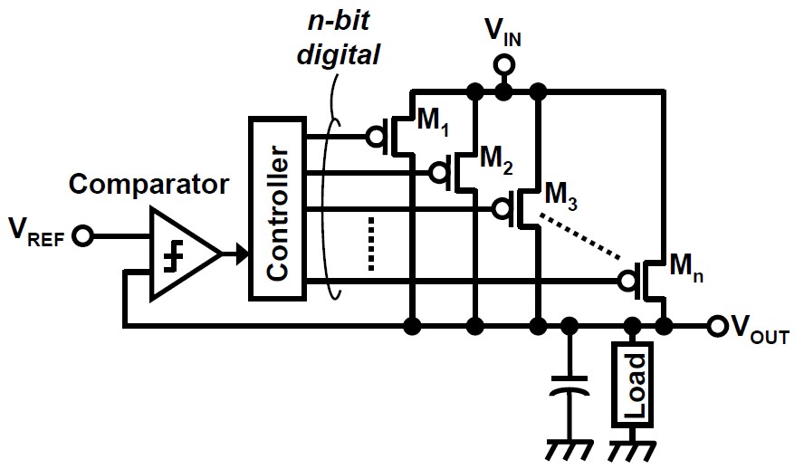
Figure 1. Digital LDO architecture [ref: Okuma et. al., CICC 2010]
The LDO_GEN tool takes in user specs (Iload,max @ Vin) and an auxiliary cell model file as inputs and outputs a behavioral verilog of the baseline Digital LDO. Below are the targeted user spec ranges (more performance specifications of the Digital LDO are added eventually as the project progresses) for which the LDO_GEN tool can output a correct design in TSMC 65nm and GF BiCMOS 8HP 130nm technology nodes:
DLDO Generator Input Spec Ranges
| Input Voltage | 0.6V – 1.3V |
| Max Load Current | 1mA – 25mA |
IDEA & POSH Integration Exercises – January 2019 Demos
Demo 1: LDO Implementation
Video 1 shows the generation of a Digital LDO design to meet an user requirement of Iload = 1mA (@ Vin = 0.7V) using the LDO_GEN tool. The design is then synthesized and placed to generate the completely placed LDO design. A parasitic extraction is done on the placed design to perform a post-parasitic extraction sim using Hspice.
Video 1: LDO_GEN tool design
Demo 2: LDO Modeling
Video 2 shows the verilog generation of test circuits for different combinations of the aux cell connections (varying number of aux cells connected in parallel at different operating voltages) in both “ON” and “OFF” states. The test verilog is then synthesized and placed to produce the test layout. Hspice simulations are performed on the post-pex netlist of the test circuits to generate an auxiliary cell model file.
Video 2: LDO_MODEL tool